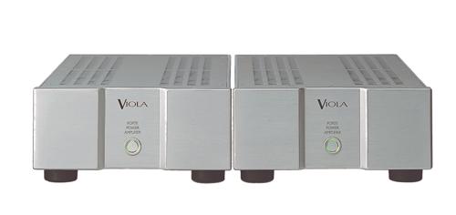
Viola Cadenza Preamplifier
$27,175.00
| Audio Design | ||
|
The Cadenza uses Class A discrete circuitry and is fully balanced throughout. The main audio circuitry is constructed on a single large mother board which accommodates the signal switching relays, local power supply sections and input and output connectors. This gives the shortest possible signal path and eliminates the variations in performance that can occur when external cable forms are used. |
||
 |
The amplification stages use Viola's custom designed OTA gainmodules. These are fully balanced and approximate to an idealized gain stage. They are constructed using discrete components, including ultra-high precision (0.1%) thin film resistors. These are employed because of their very low noise characteristic. Three types of moduleare used, each optimized for a specific application within the circuit. Careful design makes them unaffected by variations in component values. |
|
|
The input section has been designed to have an input impedance of one Meg ohm. This has three major benefits:. Each channel has an 11 position stepped gain switch for controlling channel balance. These switches can also be used to “range” input sources with atypical output levels. They are located in the inverse feedback loop for minimum noise. |
||
 |
The volume control is a custom made 59 position stepped attenuator with 1dB steps. It uses 0.1% Vishay film resistors and the contact material is a high gold content alloy also containing platinum, silver and copper. Careful design ensures that external vibration does not modulate the wiper contact pressure, as this could otherwise degrade the sound quality. To prevent ground loops between signal ended source units, all RCA inputs are completely isolated when not in use. Heavy oxygen-free copper bus bars enhance the efficiency of power distribution within the amplifier and eliminate variations that would be introduced by the use of the wiring harnesses commonly used in high performance amplifiers. |
|
| Surround Sound Processor Loop | ||
|
A switch on the mother board allows input 2 (RCA) or input 7 (XLR) or both, to be set to function as a surround sound processor (SSP) loop. If this function is not needed, these inputs may be set to function as standard stereo inputs. This approach avoids having redundant inputs when no surround sound function is required.
|
||
| Low Noise Power Supply | ||
|
The Cadenza uses a choke input filter type power supply. This produces far less Electro-Magnetic Interference than the capacitor input designs most commonly used in pre-amplifiers. It also places less stress on the power supply components, leading to higher reliability and longer life. In addition, the Cadenza's power supply design completely avoids the generation of the high frequency noise that often occurs when switch mode power supplies are used. The Cadenza's choke input power supply also virtual eliminates high peak ripple currents, thereby minimizing inter-modulation distortion on the power supply “rails” and ground returns. This further enhances the sound quality by reducing both noise and distortion. |
||
| Ease of Upgradability | ||
|
The use of plug-in modules for the gain stages allows for easy upgrading should improved versions become available in the future.
|
||
| High Quality Chassis | ||
|
The Cadenza front panel is machined from a solid aluminum slab and the side panels are custom aluminum extrusions. These are brushed to a super-fine finish and then anodized. They are mated with heavy gauge top and bottom panels to produce a structure that is extremely strong and rigid. |
||
| Warranty | ||
|
Products of Viola Audio Laboratories are warranted to be free of defects if used under normal conditions for a period of five years from the date of manufacture. |
||
| Viola Cadenza Specifications | ||
| Inputs |
1 x Option Card 4 x RCA 1 x Fischer 1 x XLR |
|
| Outputs |
1 x RCA 1 x Fischer 2 x XLR 1 x RCA (Tape) |
|
| Input Impedance | 1M ohm | |
| Frequency Response | 20Hz to 20kHz ± 0.1dB | |
| IMD | Less than 0.005% @ 1V input | |
| THD | Less than 0.01% @ 20kHz 1v input | |
| Noise | -95dB | |
| Dimensions |
Pre-amp: 44.7cm W x 9.1cm H x 40.6cm D Psu: 22.3cm W x 9.1cm H x 40.6cm D |
|
| Weights |
Pre-amp: 7.3kg Psu: 9.1kg |
|